
LDO 設計最主要的工作是設計 PMOS, error amplifer, 和適當的 frequency compenstation 電路,步驟如下:
Step 1: 由 steady state 決定 PMOS 的大小。主要是由 Iload 和 PMOS 的 Vdrop (droupout voltage) 決定,條件是讓 PMOS 維持在 saturation.

以 Iload = 50mA and Vdrop = 200mV 為例, 假設為 0.35um 3.3V 製程 uCox = 65uA/V^2. W/L ~> 40,000.
For L = 0.4um (3.3V device), W > 16mm,
WL = 6400 um^2 or 80 um x 80 um area. The gate capacitance is around 80 um x 80 um x 6 fF = 38.4 pF.
Step 2: 由 transient condition 決定 close loop (包含 error amplifier and output PMOS) 的頻寬 BW 和 Cload 的大小。
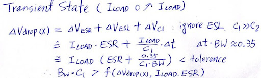
DVdrop(X) 是指在 x 點 (output point) 當 Iload 由0 跳升為 Iload 時的 voltage drop。這是由三部份所組成,ESR, ESL, and C1 的壓降。如果 ESL 很小且 Iload 不大,可忽略 ESL 的壓降。一般我們希望 DVdrop 控制在 Vout 的+/-10% 之內。因此,BW* Cload 必須大於一個常數。
( Cload * BW > constant )
先選 output cap 的大小。
Q = CV i = C dv/dt
dv = i * ESR + i / C * dt
i –> current; C –> output cap
dt –> close loop bandwidth dt * BW = 0.35 -> dt = 0.35 / BW
dv = i * ESR + 0.35 * i / (C * BW)
example: 這是由 time domain 決定。 for example, 1.2V 10% is 120mV. output current is 60mA. ESR = 0.5Ohm, vdrop = 30mV. dv = 90mv = 0.35*i / (c * BW) (c*BW) > 0.23
opamp 的 BW = 100KHz c > 3uF.
Step 3: 決定 frequency compensation 的方式
一般使用 single stage opamp 以簡化 frequency compensation 方式。因此 output pole can be obtain by Rpar * C par. Gain can be obtain gm * Rpar. Therefore, the transfer function is gm * Rpar / (1 + Rpar * Cpar * s). At high frequency, the UGF = gm / Cpar. (gm usually around 400uA/V, therefore 10M rad or 1.5MHz.
On the other hand, the output has another dominant pole, usually Gp = gmp * Rout; Cout * Rout, therefore, the UGF of output pole is gmp / Cout. assume gmp = 100mA/V, Cout = 10uF, UGF = 10K rad or 1.5kHz, far smaller compared with originally ucf.

如上所述,若沒有 compensation, 兩個 low frequency poles 會造成 no phase margin. 常見解決方法是在 output cap 上加一個 ESR zero, 但仍有其他的 output pole (usually needs to be less than 10% of output cap, Pb), 如下圖所示 。

然而 ESR 所造成的 zero, 必須小心控制,太小或太大都不合適。太大乍看之下很好,甚至可以讓 zero 和 Pa 互消,但間題是 ucf 太高, 會被下一個 pole 造成 low phase margin. 相反的,如果 ESR 太小,對 phase margin 沒有什麼貢獻。

